Our standard prototype PCBs are 2 to 8 layer PCBs with the following specifications. If your PCB has non-standard specifications, please select the corresponding items during quote and order.
| Items | Standard Process |
|---|---|
| Materials | FR4-Tg140°C |
| Fabrication Standard | IPC-A-600F Class 2 |
| Max. board size | 12” x 14”, total area <=168 sq in |
| Min. board size | |
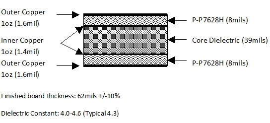
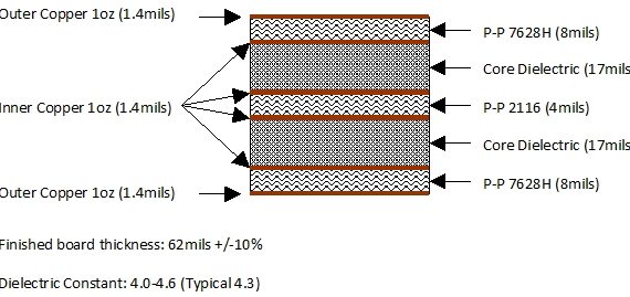
| Thickness | 0.062” |
| Copper Weight-Outer | 1oz |
| Copper Weight-Inner | 1oz |
| Finish | Hot Air Solder Leveling (HASL) |
| Outer layer min. Trace Width/Spacing | 6mil |
| Inner layer min. Trace Width/Spacing | 6mil |
| Min. Annular Ring width | 6mil |
| Min. hole size | 0.010” |
| Max. hole size | 0.200” |
| Blind/Buried vias | No |
| Min. copper to board edge clearance | >=10mil |
| Solder Mask Material | Liquid photo imageable |
| Solder mask colors | Green |
| Solder Mask sides | Both sides |
| Silkscreen material | Epoxy thermal cure |
| Silkscreen colors | White |
| Silkscreen sides | Top side or both sides if bottom side present |
| Silkscreen line width | 6mil |
| Min. letter height | 0.040” |
| Min. letter width | 0.025” |
| Impedance Control | No |
| Gold fingers | No |
| Individual routing | Individual routing |
| Irregular Outline | No more than 6 edges on board outline |
| V-score | No |
| Tab routing | No |
| Internal cut-out | No |
| Slot holes | No |
| Non-plated holes | No |
| Via tenting | No |
| Via plug | No |
| Via-in-pad | No |
| UL, Lot code, Date code | No |
We are committed to deliver you high-quality PCBs at low price. Our manufacturing facility is ISO- 9001:2000 certified and every board is inspected by a well-trained QA person. If your PCBs do not meet the specifications due to mistakes on our part, we will remake them immediately for no charge.
You can only cancel your order before it enters into “File Processing” state. If the order enters into “File Processing” state and you want to cancel it, and if it is before 6:00PM PST the same day you placed the order, you could check with us. In case the order has not entered into production, we can cancel it without any charge. If you cancel your order before we ship it, we can refund the shipping cost but all the other charges will be applied to your credit card.
If you want to place a large volume order (We provide more discount for volume orders), you can ask for a custom quote by sending your zipped Gerber 274X files and NC Drill file with a detailed description to support@PCB1STOP.com . Please include your contact information in the email. Our representative will get back to you promptly. You can also call our friendly customer representative at (713) 436-7688. If you want to place a non-standard order, please select the
non-standard specs carefully.
After you place your order online, please upload your zipped Gerber File online immediately. If you have trouble in file uploading, please email your Gerber274X files promptly to order@PCB1STOP.com , with your order number in the subject line. Please include the file name, quantity and any special requirement in the email. If there is no special requirement in the email or in online order record, the PCB board will be fabricated according our standard specs.
In order to process your order smoothly and avoid your order being on-hold, you can take the following steps to avoid the most common errors:
- Ensure all your files are readable and all needed files are included. Refer to Q8 & Q9 for the needed files. Double-check your files for design errors.
- Ensure all your files are readable and you design meets our standard specs: 0.062" thickness, 1oz copper, HASL finish, 6mil/6mil trace width/space, 12mil min. hole, 6mil min. annular ring, and 5mil min. silkscreen line width, 40mil char height etc. We recommend you to review the Gerber files and NC Drill file with free Gerber viewer ViewMate. You can download it at: http://www.pentalogix.com/Download/download.html
- Ensure Gerber files are 274-X format, not 274-D format, and the aperture list is included in Gerber 274X files. NC drill file is in ASCII format.
- Ensure the board outline is on an outline layer or any other layer.
- If you intend to use our standard specification to take advantage of online promotion prices, ensure there is no discrepancy between your fabrication notes and our standard specs. You could add “standard specs” in customer notes/comments field.
- If you have special request or your design does not meet standard specs, please include all construction information in the fabrication drawing or Read me file.
Our standard PCB prototypes are expected to have all plated holes. However, if you specify non- plated holes, we can process the order for an extra charge of $12 per order. Refer to Q16.
In Standard Prototype, we accept Gerber files in 274-X format, NC Drill files in Excellon format. If your Gerber files are in 274-D format, aperture file must be provided for each layer.
Gerber files of artwork and NC drill file are needed for PCB fabrication. For 2-layer PCB, Gerber files usually include Top Copper, Top Solder Mask, Top Silkscreen, Bottom Copper, Bottom Solder Mask, Bottom Silkscreen if needed, and outline layers if not included in the other layers; NC Drill file in Excellon format with tool sizes is needed for drilling holes; The layers corresponding to file names should be obvious, otherwise they need to be specified in the email or Readme file.
PCB’s with 4 layers or more require all file types needed for 2-layer PCB, plus the inner copper layers. The layer stack-up sequence needs to be specified in the Readme file or email.
For inner plane layers, if it is power plan or ground plan, we prefer Negative format, because it makes file size smaller, easier to transfer and process. However, if it contains circuits, you can keep it as positive layer.
No, please generate all the Gerber files seen from Top.
If you want to place the order with non-standard specs, like 2oz copper, immersion gold, please check the non-standard specs items carefully. There is small amount of extra charge for non- standard specs.
We will process the order with the special requests that you paid for. You could also ask for a custom quote by sending email to order@pcb1stop.com
Yes, we can make HDI boards with min. trace width/space of 3mils and min. hole size of 6mils. We can also make Blind/Buried via boards. Please ask for a custom quote for the special order.
Yes, we can make impedance-controlled boards. Please ask for a custom quote.
Our standard PCB prototypes are expected to have all holes plated. However, if you choose non- plated holes in your online order or custom order, we can process orders with non-plated holes with an extra charge of $12 per order. Please have the non-plated holes defined clearly in your zipped Gerber file or readme file.
Yes, we have green, red, blue, black, and white solder masks. There is an extra charge of $20 per order for solder masks other than green.
Yes, we have red, blue, and white silkscreen colors. There is an extra charge of $20 per order for silkscreen colors other than white.
In our standard Prototype, the board thickness is 62 mils. We can also make boards with thickness of 24 mils, 31 mils, and 47 mils with an extra charge of $30 per order, and boards with thickness of 78 mils or above with min. extra charge of $40 for 2-layer prototype, depending on the total area size.
In our standard Prototype, finished copper weight is 1oz inner/1oz outer. We can also make boards with copper weight of ½oz, 2oz, and 3oz. There is an extra charge of $20 for ½oz and min. extra charge of $30 per order for 2oz copper, and $60 for 3oz copper, depending on the total area size.
There is an extra charge of $50 or more for Immersion Gold finish, and $30 for Lead Free finish, depending on the total board area.
There is min. extra charge of $50 per order for Gold Fingers plating.
If you need both side silkscreens, we can make it for you free. You need to choose two sides silkscreen when you place the order.
Yes, we can make internal routing. If it is very simple internal cut-out we will make it for you free of charge. Please make sure to add “internal cut-out needed” in customer notes/comments field.
There will be an extra charge of $30 or more per order for complicated internal routing.
We can make up to 5 slot holes for you free if you clearly draw them in the design files and the slot hole width needs to be at least 40mils. If there are more than 5 slot holes, there will be an extra charge of $30 or more per order, depending on the total price.
Yes, we can make tab routing; there will be an extra charge of $50 or more per order, depending on the complexity.
In general, the standard online prices do not apply to orders with multiple images or Step & Repeat. If you place an order with Multiple Images or Step & Repeat on the layout, there will be an extra charge, depending on the number of layers and images, in addition to the total board price, e. g. $30 for each additional image or Step & Repeat for 2-layer board. You could also request a custom quote by sending email to order@pcb1stop.com
Please understand that all the prototype boards involve file review, setup, film making, and more than 20 steps of process. It takes extra work to process an order with multiple images. We don’t encourage designs with multiple images, but if you want to save some money, we can make it for you with a little compensation.
Yes, there is an extra charge of $50 per order for panel with V-cut and $30.00 per order for panel without V-cut. The Min. panel size is 0.44" x 0.4", Max. Panel size is 16" x 10", Min. Groove to Groove width is 0.4"; V-cut angle is 45 degrees; Groove width is 20mils, V-cut should be from edge to edge (No jump scoring). If you don't know how to make the best way for V-cut, you could send the single Gerber file to us and we will make it for you.
The drill sizes in the NC drill file are finished hole sizes. The actual tool sizes we use are approx. 2 mils larger than the finished hole sizes since there is approx. 1 mil thick copper-plated wall in the holes.
Finished drill sizes from 10 mils to 22 mils with step of 4 mils, from 24 mils to 44 mils with step of 2 mils, and from 48 mils to 240 mils with step of 4 mils. For hole size larger than 240 mils, we use routing instead of drilling, the tolerance is +/- 3mils. But no more than10 of holes larger than 240mils are allowed on a single board. Boards with finished hole sizes smaller than 10mil and larger than or equal to 8 mil will considered as high density board (HDI), and there is an extra charge for HDI.
If the finished hole size is not the exact size we can make, we will round it up to the closest one with maximum deviation of 2 mils. Usually the difference can be neglectable. As long as your hole sizes are within the specified range, usually there is no problem with it.
PCB1STOP will hold every customer's design files and other confidential information in strict confidence. We will not disclose such files and confidential information to any third parties, and will not use such files and confidential information for any purpose except for the customer’s PCB fabrication.
Our standard turn times are 5 business days for 2-layer PCB, 7 days for 4-layer PCB, 8 days for 6-layer PCB, 8 days for 8-layer PCB, and 10 days for 10-layer PCB. We also offer expedited turn time with extra charge. Expedited turn times are 3 days for 2-layer PCB, 5 days for 4-layer PCB, 5 days for 6-layer PCB, 6 days for 8-layer PCB, and 8 days for 10-layer PCB. If you want turn time faster than the expedited turn time, please send your request to order@pcb1stop.com. Please include your Gerber file, turn time desired, quantity an any non-standard specs in your email. Please make sure your Gerber files are correct. We make your boards based on your design files. In case we find obvious and significant errors, we will contact you and the turn time will be counted from the day when problems are solved.
We calculate the turn time from the cut-off time, which is 6:30 PM Central Time on each business day. For example, if you have a 5 day turn time order that comes in on Tuesday before 6:30 PM, then your order will be shipped on the next Tuesday if there is no holiday during the turn time. If the total area size>=3,100 in^2 or Qty > 500pcs, the standard turn tie will be 10-day up for 2 & 4 layer PCB; adn15-day up for 6 &8 layer PCB.
(International Traffic in Arms Regulations) U.S. State Department regulations that govern the export of restricted technology to foreign states other than Canada. If your board design data is ITAR-controlled, please inform us before you place your order. For more information on ITAR, please go to http://en.wikipedia.org/wiki/ITAR or http://pmddtc.state.gov/.
9:00AM to 6:00PM PST, Monday through Friday.
Currently we use FedEx for order shipping to the US or Canada. The starting shipping charge of 1Lb is $25 to the US and $28 to Canada. It is overnight shipping to most of the cities in continental states in US and Canada.
Send email to support@pcb1stop.com or call customer service at (713) 436-1000.
1, FAQ for PCB fabrication:
Lorem ipsum dolor sit amet, consectetur adipiscing elit. Aliquam in felis mattis, dignissim mauris non, sodales mauris. Mauris pellentesque ultricies quam a ultrices. Sed id cursus lorem, ut suscipit eros. Donec varius sem sed pellentesque dignissim. Donec accumsan sed nulla sollicitudin fermentum.
Aliquam eget diam vestibulum, volutpat tortor vel, tempor tortor. Lorem ipsum dolor sit amet, consectetur adipiscing elit. Vivamus non augue blandit, mattis velit a, efficitur ex. In hac habitasse platea dictumst. Morbi blandit eget ipsum eu consectetur. Phasellus id varius augue.
Aliquam eget diam vestibulum, volutpat tortor vel, tempor tortor. Lorem ipsum dolor sit amet, consectetur adipiscing elit. Vivamus non augue blandit, mattis velit a, efficitur ex. In hac habitasse platea dictumst. Morbi blandit eget ipsum eu consectetur. Phasellus id varius augue.
Vivamus pulvinar risus vel turpis pellentesque sollicitudin. Praesent nec lacus at purus fringilla maximus id in tortor. Suspendisse vel dictum velit. Sed consectetur congue odio, ornare cursus nisi lacinia vel. Curabitur sit amet tempus elit, sed tempus elit. Mauris varius elit at bibendum tincidunt.
Morbi at nisi eget nunc posuere mollis quis ut augue. Vestibulum vitae facilisis erat. Aenean velit purus, interdum a facilisis at, tincidunt at nisl. Mauris sit amet dictum arcu. Sed faucibus nunc eget ultrices commodo. Integer id diam nec magna blandit blandit non at massa. Morbi dictum ac tortor eget vehicula. Nam vulputate varius nisi egestas fringilla. Curabitur mi tortor, vehicula sed tempor ut, dapibus ac eros.
Vestibulum eros sem, tristique nec lacus nec, viverra sollicitudin lorem. Nam et ligula placerat, molestie lorem vel, sollicitudin erat. Vestibulum rutrum mauris eu justo mollis, at fringilla nunc consequat. Maecenas ac efficitur elit. Nulla vehicula ante in nisl placerat, vitae elementum tellus vehicula. Mauris a ipsum sagittis, finibus metus ut, scelerisque eros. Nulla pretium mauris eget turpis ultricies malesuada.
2, FAQ for PCB Assembly:
Lorem ipsum dolor sit amet, consectetur adipiscing elit. Aliquam in felis mattis, dignissim mauris non, sodales mauris. Mauris pellentesque ultricies quam a ultrices. Sed id cursus lorem, ut suscipit eros. Donec varius sem sed pellentesque dignissim. Donec accumsan sed nulla sollicitudin fermentum.
Aliquam eget diam vestibulum, volutpat tortor vel, tempor tortor. Lorem ipsum dolor sit amet, consectetur adipiscing elit. Vivamus non augue blandit, mattis velit a, efficitur ex. In hac habitasse platea dictumst. Morbi blandit eget ipsum eu consectetur. Phasellus id varius augue.
Suspendisse ultricies nunc a tempor lacinia. Duis ullamcorper massa libero, et vehicula justo dignissim et. Maecenas vel sem ultrices, pulvinar augue sed, vulputate risus. Vestibulum faucibus, lorem eget pulvinar convallis, turpis mauris scelerisque velit, eu condimentum risus justo quis lacus. Nam at leo orci. Proin pharetra felis eu viverra molestie. Praesent efficitur porttitor erat blandit bibendum. Etiam neque mi, ullamcorper et blandit ac, scelerisque at turpis. Cras lobortis a lorem ac venenatis.
Vivamus pulvinar risus vel turpis pellentesque sollicitudin. Praesent nec lacus at purus fringilla maximus id in tortor. Suspendisse vel dictum velit. Sed consectetur congue odio, ornare cursus nisi lacinia vel. Curabitur sit amet tempus elit, sed tempus elit. Mauris varius elit at bibendum tincidunt.
3, FAQ for PCB Layout
Lorem ipsum dolor sit amet, consectetur adipiscing elit. Aliquam in felis mattis, dignissim mauris non, sodales mauris. Mauris pellentesque ultricies quam a ultrices. Sed id cursus lorem, ut suscipit eros. Donec varius sem sed pellentesque dignissim. Donec accumsan sed nulla sollicitudin fermentum.
Aliquam eget diam vestibulum, volutpat tortor vel, tempor tortor. Lorem ipsum dolor sit amet, consectetur adipiscing elit. Vivamus non augue blandit, mattis velit a, efficitur ex. In hac habitasse platea dictumst. Morbi blandit eget ipsum eu consectetur. Phasellus id varius augue.
Suspendisse ultricies nunc a tempor lacinia. Duis ullamcorper massa libero, et vehicula justo dignissim et. Maecenas vel sem ultrices, pulvinar augue sed, vulputate risus. Vestibulum faucibus, lorem eget pulvinar convallis, turpis mauris scelerisque velit, eu condimentum risus justo quis lacus. Nam at leo orci. Proin pharetra felis eu viverra molestie. Praesent efficitur porttitor erat blandit bibendum. Etiam neque mi, ullamcorper et blandit ac, scelerisque at turpis. Cras lobortis a lorem ac venenatis.
Vivamus pulvinar risus vel turpis pellentesque sollicitudin. Praesent nec lacus at purus fringilla maximus id in tortor. Suspendisse vel dictum velit. Sed consectetur congue odio, ornare cursus nisi lacinia vel. Curabitur sit amet tempus elit, sed tempus elit. Mauris varius elit at bibendum tincidunt.
Vivamus pulvinar risus vel turpis pellentesque sollicitudin. Praesent nec lacus at purus fringilla maximus id in tortor. Suspendisse vel dictum velit. Sed consectetur congue odio, ornare cursus nisi lacinia vel. Curabitur sit amet tempus elit, sed tempus elit. Mauris varius elit at bibendum tincidunt.